Perovskite Solar Cells Prepared by Advanced Three-Step Method Using Additional
HC(NH2)2I Spin-Coating: Efficiency Improvement with Multiple Bandgap Structure
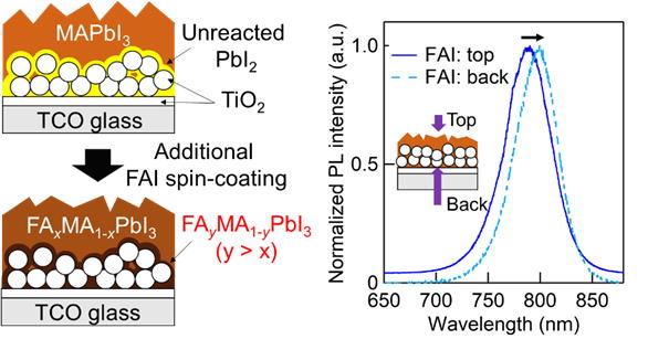
In the conventional two-step prepared perovskite solar cells, the CH3NH3PbI3 (MAPbI3) film usually contains an unreacted PbI2 at the interface between an electron transport layer (ETL) and a perovskite active layer. To reduce the unreacted PbI2 in the two-step prepared MAPbI3
film, we have recently reported a new three-step method, which was
realized by an additional MA(I,Br) spin-coating. Here, we propose an
advanced three-step method, viz., an additional HC(NH2)2I (FAI) spin-coating on the two-step prepared MAPbI3 film. The additional FAI spin-coating formed a FAxMA1‐xPbI3 solid solution by the incorporation of FA ion into MAPbI3. Also, the additional FAI spin-coating yielded a FAyMA1-yPbI3 layer (y > x) by converting the unreacted PbI2,
which resulted in the layered structure with different FA
concentrations and hence, with the multiple bandgap structure. The best
PCE of 18.1% was achieved by optimizing the FAI spin-coating process.
HC(NH2)2I追加スピンコーティングを用いる先進3ステップ法により作製したペロブスカイト太陽電池:マルチバンドギャップ構造による効率改善
従来の2ステップ法で作製したペロブスカイト太陽電池では、CH3NH3PbI3 (MAPbI3)膜は、通常、電子輸送層(ETL)とペロブスカイト活性層との界面に未反応のPbI2を含んでいる。 2ステップ法で調製したMAPbI3膜中の未反応PbI2を減少させるために、我々は最近、新たな3ステップ法を報告した。これはMA(I,Br)追加スピンコーティングにより実現したものである。
本研究では、2ステップ法で調製したMAPbI3膜上に、HC(NH2)2I (FAI)追加スピンコーティングを施した先進3ステップ法を提案する。 FAI追加スピンコーティングにより、MAPbI3へのFAイオンの取り込みによってFAxMA1-xPbI3固溶体が生成した。 また、FAI追加スピンコーティングは、未反応PbI2を変換することによってFAyMA1-yPbI3層(y>x)を生成し、これによってFA濃度の異なる層状構造、すなわち多重バンドギャップ構造をもたらした。さらに、FAIスピンコーティングプロセスを最適化することにより、最高18.1%の光電変換効率が達成できた。
|
 |
Y. Okamoto, T. Yasuda, M. Sumiya and Y. Suzuki, ACS Appl. Energy Mater., 1 [3] 1389-1394 (2018).
https://doi.org/10.1021/acsaem.8b00178 |
|
Perovskite solar cells with CuI inorganic hole conductor
An organic material, 2,2',7,7'-tetrakis(N,N-di-p-methoxyphenylamine)9,9'-spirobifluorene
(spiro-OMeTAD), is generally used as a hole conductor of perovskite solar
cells (PSCs), but spiro-OMeTAD is much more expensive than other materials
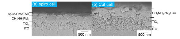
used in PSCs. In this study, we have prepared PSCs with a cost-effective
CuI hole transport layer by spin coating. The merit of using spin coating
for CuI is good compatibility with other steps, such as spin coating of
a TiO2 electron transport layer and a
perovskite active layer. The CuI-based PSC recorded power conversion
efficiencies of η = 2.22% (max) on the day of production and η = 6.52%
(max) after the 20 days of production. Moreover, the CuI-based PSC had a
smaller hysteresis than the spiro-based PSC, suggesting that CuI is a
highly promising alternative hole conductor for PSCs.
CuI無機ホール導体を有するペロブスカイト太陽電池
有機材料であるspiro-OMeTADは、ペロブスカイト太陽電池(PSC)のホール伝導体として一般に使用されるが、spiro-OMeTADはPSCで使用される他の材料よりもはるかに高価である。
本研究では、費用対効果に優れたCuI正孔輸送層を有するPSCをスピンコーティングによって作製した。 CuIの成膜にスピンコーティングを使用する利点は、TiO2電子輸送層およびペロブスカイト活性層のスピンコーティングなどの他のステップとの良好な適合性を有することである。
CuIベースのPSCは、作製日に最大でη= 2.22%、作製後20日目に最大でη= 6.52%の変換効率を記録した。 さらに、CuIベースのPSCは、spiroベースのPSCよりもヒステリシスが小さく、CuIがPSC用の有望な代替ホール伝導体であることを示唆した。 |
 |
K. Takahashi and Y. Suzuki, Jpn. J. Appl. Phys., 56, 08MC04 (2017).
https://doi.org/10.7567/JJAP.56.08MC04 |
|
|
Copyright (c) 2011-2018 Yoshikazu Suzuki Laboratory, University of Tsukuba
|
|
